

Learning about its optical properties
Graphene – a thin membrane formed by one or two atom-thick layers of carbon – is considered one of the future building blocks of nanotechnology. Gaining tremendous attention in the last years, graphene and graphene-based material combinations such as graphene/boron nitride find potential applications in optical and opto-electronic devices. To design new optical devices, we have to understand how the material interacts with its surrounding, especially with the material the graphene is deposited on.
In a joined effort, scientists of the Brazilian Nanotechnology National Laboratory (LNNano), the Brazilian Synchrotron Light Source (LNLS) and from the Federal University of Minas Gerais (UFMG), investigated the optical properties of graphene lying on a boron nitride and a silicon dioxide substrate.
The researchers used the newly built infrared beam line at the LNLS setup by R. Freitas and F. Barbosa. There are very few infrared beamlines with this special powerful equipment in the world, so this was a unique opportunity to investigate these materials. The infrared beam line allows the characterization of the material with a lateral resolution of 50 nm – which is roughly 1000 times better than with a more common infrared optical microscope. Not only can the researchers obtain very high resolution images, but they can also probe the interaction of the graphene with the underlying material by carrying out infrared spectroscopy.

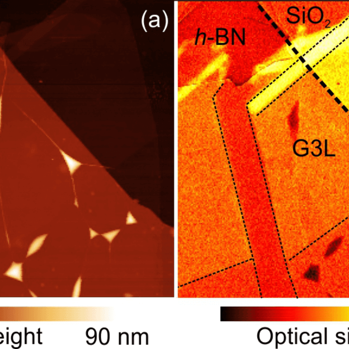
Figure (a) shows the nanometric topography of a boron nitride (left side) with a graphene layer on top extending over the edge of the boran nitride to the right. (b) Infrared image with an ultra high resolution obtained by the unique instrumentation of the LNLS beamline. The graphene layer shows up in the image by its stronger optical signal.
Published in the journal Nanoscale of the Royal Chemical Society of England, the figure above shows highly resolved images of a sample. The figure (a) depicts the nanometric topography of the sample obtained by scanning a very fine probe over the surface of the sample. The left side of the image (a) shows boron nitride with single and triple atom thick graphene layers lying on top. The graphene layers extend over the edge of the boron nitride and lay partly on silicon dioxide substrate. This is also seen on the right side of the image (a).
Image (b) above shows the infrared image obtained at the LNLS beamline. The color difference in the parts of the image show the optical response of the graphene, which is different for the number of layers (3 or 1) as well as for the underlying substrate (the brighter areas are the graphene lying on the silicon dioxide). Finally, dark spots are seen where the graphene separates from the underlying substrate. Hence, when the contact is broken, the optical response of the graphene is much weaker.
Corresponding author of the work, Christoph Deneke working at the LNNano and speaking for the team, explains that these investigations together with the obtained infrared spectra from the graphene/boron nitride extend our basic understanding of the material system.
“Seeing these results shows us that the optical properties of the graphene depend on the underlying substrate”, he explains. “We learn that unlike for common materials used for optical devices, for our nanometer thin graphene it matters, what is below it. And, we see that the graphene interacts with the material below it – the optical activity is much higher on the silicon dioxide than on the boron nitride. But both materials enhance the optical activity compared to the pure graphene as we learned from the bubbles.”
The spectroscopy data provided a detail image of the graphene interaction with the support layer, showing that the specific material vibrations of the underlying substrate are responsible for the different optical properties of the graphene. The research team hopes that with further experiments using this powerful and unique facility, they can further understand the optical behavior of the graphene and optimize it for the integration into future devices like sensors for infrared light, flat displays and TV or solar cells.
Source: I.D. Barcelos, A.R. Cadore, L.C. Campos, A. Malachias, K. Watanabe, T. Taniguchi, F.C. Maia, R. Freitas, C. Deneke. Graphene/h-BN plasmon–phonon coupling and plasmon delocalization observed by infrared nano-spectroscopy. Nanoscale, 2015,7, 11620-11625. doi:10.1039/C5NR01056J
Research can lead to new treatments against envenoming
The results, by CNPEM researchers, were published in the journal “Scientific Reports” from Nature Group.