CONTACT & STAFF
Facility Tel.: +55 19 3518 2574
Facility E-mail: lcis@lnls.br
Coordination: Pedro S. de N. Muniz
Tel.: +55 19 3512 1051
E-mail: pedro.schio@lnls.br
Click here for more information on this Facility team.


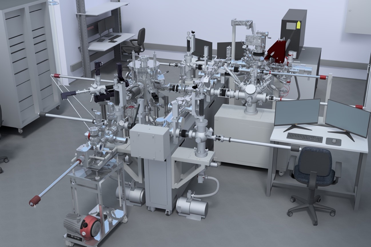
The in-situ growth laboratory offers to user tools at the state of the art for the growth of thin films and heterostructures for posterior studies with synchrotron radiation. The growth techniques available are based on physical vapor deposition on two modes: Pulsed Laser Deposition (PLD) and Molecular Beam Epitaxy (MBE). Thin films of different materials can be produced from transition metals, its oxides and small organic molecules. The growth chambers are coupled via an ultra-high vacuum (UHV) tunnel and permit the samples to be transferred between the chambers without air exposure. There is also the possibility of growing thin films and transport them to the beamlines also in UHV conditions (via vacuum suitcase), which is essential for the study of surfaces.
Facility Tel.: +55 19 3518 2574
Facility E-mail: lcis@lnls.br
Coordination: Pedro S. de N. Muniz
Tel.: +55 19 3512 1051
E-mail: pedro.schio@lnls.br
Click here for more information on this Facility team.
Molecular Beam Epitaxy is a technique for the deposition of thin films with high crystallographic quality and purity over adequate substrates. The technique is based on heat a given material to produce an atomic/molecular beam which, due to the UHV conditions of the chamber, can translate in the chamber until reach a substrate and be incorporated. The growth rates are small allowing the growth control in the molecular layer range.
On LCIS there are two growth chambers dedicated to this technique: (i) one for the growth of transition metals (or materials with low vapor pressure) and (ii) other chamber adapted for growing small organic molecules.
The chamber operates with a base pressure of 10-10 mbar, is equipped with 10 e-beam evaporators, has a quartz balance for calibration of growth rate. Also is possible to use an Argon beam for sputter substrates for cleaning the surface, and to heat the substrate through electron bombardment. The substrates and thin films can be characterized in-situ by electron diffraction in two different geometries, LEED and RHEED, allowing to follow the growth layer by layer. The system also contains a motorized mask which allows the partial deposition, atomic steps or even linearly dependent thickness.
LCIS has available a deposition chamber equipped with a Knudsen evaporator for deposition of small organic molecules. On this chamber the substrate can be heated up to 500°C and there is a possibility to use masks for select the area of deposition. Also, it is possible for users to bring their own evaporators for deposition of previously accepted materials.
Pulsed Laser Deposition is a technique for producing thin films that use a high-power pulsed laser for vaporize and ionize material from a target. Once the laser impinges the target, a plume is created and directed to a substrate. This plume is composed of ions, electrons and neutral particles and, in some conditions, can maintain the target stoichiometry. The stoichiometry conservation possibility is the principal differential of this technique. Also, PLD is a versatile technique that enable to growth films with controlled atmosphere from vacuum up to mbar range. The technique has been used for the growing of different materials as cuprate superconductors and ferroelectric and ferromagnetic oxides.
At LCIS there is available a chamber for deposition via pulsed laser deposition that uses a Excimer laser of KrF with wavelength of 248nm, maximum energy per pulse 400mJ and repetition rate 20Hz. The deposition chamber is equipped with a carrousel containing up to 6 targets of one-inch diameter by 3 to 6 millimeters of thickness. The substrate can be heated via infrared laser heating up to 850°C. The deposition process can be performed at pressure between 1e-8mbar up to 1mbar pressure range with Nitrogen, Argon or Oxygen atmosphere. The chamber has a quartz balance para calibrate the deposition rate and an electron gun allowing to follow the growth via RHEED. The users can bring their own targets with chemical composition previously accepted (highly volatile atoms – Pb, K…- are forbidden).
LCIS offers to users some pre-characterization of films. Beside the accessory techniques connected to growth chambers as LEED and RHEED the laboratory has possibility of determining the surface morphology of films growth through scanning probe microscopy techniques and also the possibility of measure electrical transport properties.
The surface morphology of substrates and thin films can be investigated through scanning probe microscopy. For that, a small probe with sharp edge is scanned very close the sample surface. In Scanning Tunneling Microscopy (STM) is detected the tunneling current between probe and conducting sample. This current is only significant when the distance is very small. In Atomic Force Microscopy (AFM) the probe is also at very small distance from the surface in conditions that the resultant forces of interaction between probe and the atoms at sample surface are relevant.
LCIS is equipped with two microscopes to offer to the users. One of them operates at ultra-high vacuum conditions and is attached to growth chambers through vacuum tunnel. It is a NANONIS microscope using KolibriSensor form SPECS which allows measure in AFM and STM mode. The chamber also permits to heat samples via e-beam heater and to sputter samples with Argon.
The other microscope operates at ambient pressure. It is a NanoSurf FlexAFM with possibility for operation on the modes of Atomic Force Microscopy, PiezoResponse Force Microscopy, Magnetic force Microscopy and Kelvin-probe force microscopy.
A cryostat has been adapted in a vacuum chamber for allowing measurements of electronic transport of thin films produced. The cryostat base pressure is on the 10-6 mbar and sample temperature in the range between 15K e 320K. Near the sample holder there is 8 electrical contacts that can be connected to sample for performing measurements. The system is equipped with a source Keithley 6430 and a nanovoltmeter for performing curves of current versus bias in fixed temperatures or to measure resistance in function of temperature with constant bias or current.