CONTACT & STAFF
Facility Tel.: +55 19 3517 5140
Coordination: Ingrid D. Barcelos
Tel.: +55 19 3518 2517
E-mail: ingrid.barcelos@lnls.br
Click here for more information on this Facility team.


The Microscopic Samples Laboratory (LAM) acts as a support laboratory for beamlines, whose main purpose is advanced sample preparation. The LAM infrastructure is divided into two sectors: Electronic Microscopy and Optical Microscopy Laboratory, both facilities offer tools for both sample production and characterizations complementary to the experiments in the beamlines.
Facility Tel.: +55 19 3517 5140
Coordination: Ingrid D. Barcelos
Tel.: +55 19 3518 2517
E-mail: ingrid.barcelos@lnls.br
Click here for more information on this Facility team.
 Specifications
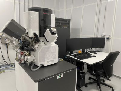
Dual-beam electron microscope that combines a focused ion-beam microscope (FIB) and a scanning electron microscope (SEM). It has an electron gun with accelerating voltage between 350V and 30kV and a Xe+ plasma gun with accelerating voltage between 500V and 30kV, eliminating sample contamination by Ga+. It allows the acquisition of images of secondary electrons (SE) and transmitted (STEM) with resolutions up to 0.6 nm. It has detectors of Energy Dispersion X-ray Spectroscopy (EDS), Electron Backscattered Diffraction (EBSD), and Cathodoluminescence. It has a nano manipulator and a gas injection system (GIS) for deposition of materials, cross-sections, and micro-machining, in addition to the preparation of high-quality samples for Tomography and Transmission Electron Microscopy (TEM). As it achieves low acceleration voltages, up to 500V, it makes it possible to perform a final polish with low-energy ions, improving the quality of the samples produced. Besides, 3D images can be obtained in an automated way through sequential cuts.
Techniques
Imaging Modes
SEM Techniques
FIB Techniques
 Specifications
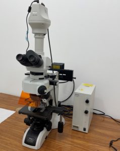
The Nikon Eclipse LV100ND Optical Microscope allows imaging at magnifications of 5x, 20x, 50x, and 100x in brightfield and darkfield with reflected (episcopic) and transmitted (diascopic) illumination from LV-LH50PC light sources. In addition, it has a C-HGFI mercury light source for high-quality fluorescence images with uniform brightness. For image capture and processing, the microscope is equipped with a DS-Ri2 digital camera, enabling the use of the NIS-Elements Documentation software, which provides basic measurement and report creation tools.
Techniques
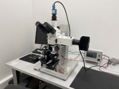
The HQ Graphene transfer system is used to fabricate Van der Waals heterostructures, allowing precise stacking of atomic layers. For this, the system provides a high degree of freedom in the x, y, and z axes and tilting and rotational movements. It has an optical microscope with a maximum magnification of 50x and a CCD camera for viewing the samples.