CONTACT & STAFF
For more information on this beamline, contact us.
The IR1 beamline is an endstation dedicated to infrared nanospectroscopy (nano-FTIR) in the range of mid-IR. Its main purpose is the analysis of chemical-optical properties of condensed matter in the nanoscale. In similar fashion to established infrared spectroscopy (FTIR), the nano-FTIR allows for identification and characterization of a chemical compound by means of its vibrational response, however, with nanoscale spatial resolution. Moreover, nano-FTIR is a technique based on near-field optics and, therefore, can be applied to the optical analysis in the sub-diffractional regime of plasmonic and photonic materials.
To overcome the diffraction limit of light, this experimental endstation uses the broadband synchrotron IR beam extracted from the LNLS storage ring as the light source for the experiment Scattering Near-Field Optical Microscopy (s-SNOM). In this experiment a metal coated atomic force microscopy (AFM) tip acts as an antenna for the light confinement at the its apex, creating a new source that no longer depends on the incident light wavelength but it is defined by the shape of the AFM probe, allowing for a spatial resolution of c.a. 25 nm.
The specifications of IR1 beamline of LNLS allows for multidisciplinary studies in Physics, Chemistry and Biology, in particular those studies in which the local chemical information is the central point in the research.
Potential applications are: Opto-electronics and vibrational properties of 2D materials, chemical analysis of sub-micron molecular domains in polymer blends, nano-drugs delivery, single cell chemistry, vibrational analysis of archeological micro-artefacts, new nanostructured materials for energy harvesting and conversion.
For more information on this beamline, contact us.
The IR1 beamline is exclusively dedicated to the Scattering Near Field Optical Microscopy technique (s-SNOM) which associates infrared microscopy (μ-FTIR) and atomic force microscopy (AFM). To learn more about the techniques’ limitations and requirements (sample, environment, etc.) contact the beamline coordinator before submitting your proposal.
scattering Scanning Near-Field Optical Microscopy (s-SNOM) is a nanoscopy technique which combines Atomic Force Microscopy (AFM) and optics for producing a tip-enhanced optical or infrared (IR) probe with spatial resolution beyond the diffraction limit of light. In the case of the IR1 beamline, the broadband synchrotron IR beam is focused on a metallic AFM tip (nano-antenna) generating a broadband source smaller than 40 nm. The interaction of the IR nano-source with the sample surface yields broadband images (scanning mode) or 40 nm pixel point spectrum.
Recent publications:
B. Pollard et al. (2016). Infrared Vibrational Nanospectroscopy by Self-Referenced Interferometry. Nano Letters, vol. 16, 55–61. doi: 10.1021/acs.nanolett.5b02730
I. Barcelos et al. (2015). Graphene/h-BN Plasmon-phonon coupling and plasmon delocalization observed by infrared nano-spectroscopy. Nanoscale, vol.7, 11620–11625. doi: 10.1039/C5NR01056J
T. Moreno et al. (2013). Optical layouts for large infrared beamline opening angles. Journal of Physics: Conference Series, 425(14), 142003. doi:10.1088/1742-6596/425/14/142003
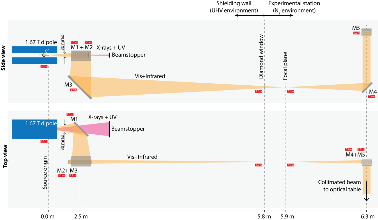
| Element | Type | Position [m] | Description |
|---|---|---|---|
| SOURCE | Bending Magnet | 0.0 | Bending Magnet D03 exit A (4°), 1.67 T, 30 mrad x 80 mrad |
| M1 | Plane, 6 mm slot | 2.5 | Gold coated, aluminum substrate |
| M2 | Tangential cone-shaped | 3.1 | Gold coated, aluminum substrate |
| M3 | Tangential cylinder | 3.7 | Gold coated, aluminum substrate |
| CVD | Diamond window | 7.0 | 20 mm diameter by 500 µm diamond window by Chemical Vapor Deposition |
| M4 | Tangential cylinder | 7.5 | Gold coated, aluminum substrate |
| M5 | Tangential cylinder | 7.9 | Gold coated, aluminum substrate |
| Parameter | Value | Condition |
|---|---|---|
| Energy range [cm-1] | 3000 – 700 | Broadband radiation limited by beamsplitter transmission and detector sensitivity |
| Energy resolution [cm-1] | Up to 3.3 | Limitted by the interferometer travel |
| Beam size at sample [nm, FWHM] | < 40 nm | Near-field spot defined by the size of the s-SNOM tip |
| Flux at first optical element [Phot/s/0.1%bw] | 2.0 x 10¹³ | at 1000 cm-1 (10 µm) |
| AFM scanning stage (maximum travel) [µm] | ± 45 | – |
| AFM scanning stage minimum step [nm] | 5 | – |
| Instrument | Type | Model | Manufacturer | Specifications |
|---|---|---|---|---|
| s-SNOM | Near-field Optical Microscope | NeaSnom | – | NeaSpec |
| MCT Detector | Single element Mercury-Cadmium-Telluride (MCT) | KLD-0.1-J1208L | 750 cm-1 to 3000 cm-1, 100 µm element size, DC to 1 MHz BW, LN2 cooled | Kolmar Technologies |
| MCT Detector | Single element MCT | IRA-20-00103 | 650 cm-1 to 3000 cm-1, 50 µm element size, 500 Hz to 2 MHz BW, LN2 cooled | Infrared Associates Inc. |
| Si Detector | Single element Silicon detector | PDA36A-EC | 350 nm to 1100 nm, 3.6 mm x 3.6 mm element size, DC to 10 MHz BW , air cooled | Thorlabs |
| InGaAs Detector | Single element Indium-Gallium-Arsenide (InGaAs) detector | PDA10D-EC | PDA10D-EC | Thorlabs |
| Lock-in amplifier | 2 input channels digital lock-in amplifier | HF2LI | DC to 50 MHz, 210 MSa/s, USB 2.0 high-speed, 480 Mbit/s | Zurich Instruments |
| Visible laser | HeNe laser | HNL150L | 15 mW HeNe (633 nm) laser | Thorlabs |
Data acquisition is performed directly in the native software of the NeaSnom microscope developed by Neaspec. S-SNOM image files are compatible with the free program Gwyddion (http://gwyddion.net) and point spectra, linescans and spectral images are postprocessed using Mathematica® routines developed by the IR1 team.
Users are required to acknowledge the use of LNLS facilities in any paper, conference presentation, thesis and any other published material that uses data obtained in the execution of their proposal.
Scattering Scanning Near-field Optical Microscopy (s-SNOM)
Keilmann, F. & Hillenbrand, R. Near-field microscopy by elastic light scattering from a tip. Trans. A. Math. Phys. Eng. Sci. 362, 787–805 (2004).
Huth, F., Schnell, M., Wittborn, J., Ocelic, N. & Hillenbrand, R. Infrared-spectroscopic nanoimaging with a thermal source. Mater. 10, 352–6 (2011).
Huth, F. et al. Nano-FTIR absorption spectroscopy of molecular fingerprints at 20 nm spatial resolution. Nano Lett. 12, 3973–8 (2012).
Muller, E. A., Pollard, B. & Raschke, M. B. Infrared Chemical Nano-Imaging: Accessing Structure, Coupling, and Dynamics on Molecular Length Scales. Phys. Chem. Lett. 6, 1275–1284 (2015).
Infrared Spectroscopy Espectroscopia de Infravermelho (FTIR)
Griffiths, P. R. & de Haseth, J. a. Fourier Transform Infrared Spectrometry. Chemical Analysis: A Series of Monographs on Analytical Chemistr and Its Applications (2007). doi:10.1002/047010631X
Smith, Brian C. “Fourier transform infrared spectroscopy.” CRC, Boca Raton, FL(1996).
Atomic Force Microscopy Microscopia de Força Atômica
Eaton, P. & West, P. Atomic Force Microscopy. (Oxford University Press, 2010). doi:10.1093/acprof:oso/9780199570454.001.0001
Scientific publications produced with data obtained at the facilities of this beamline, and published in journals indexed by the Web of Science, are listed below.
Codeço, C. F. S. ;Barcelos, I. D.;Mello, S. L. de A. ;Penello, G. M. ;Magnani, B. da F.. Superficial Si nanostructure synthesis by low-energy ion-beam-induced phase separation, Applied Surface Science, v.601, p. 154190, 2022. DOI:10.1016/j.apsusc.2022.154190
Oliveira, R. de;Guallichico, L. A. G. ;Policarpo, E.;Cadore, A. R.;Freitas, R. O.;Silva, F. M. C. da ;Teixeira, V. C.;Magalhães-Paniago, R.;Chacham, H.;Matos, M. J. de S.;Malachias, A.;Krambrock, K.;Barcelos, I. D.. High throughput investigation of an emergent and naturally abundant 2D material: Clinochlore, Applied Surface Science, v.599, p. 153959, 2022. DOI:10.1016/j.apsusc.2022.153959
Grasseschi, D.;Bahamon, D. A.;Maia, F. C. B.;Barcelos, I. D.;Freitas, R. O.;Matos, C. J. S. de. Van der Waals materials as dielectric layers for tailoring the near-field photonic response of surfaces, Optics Express, v.30, n.1, p.255-264, 2022. DOI:10.1364/OE.445066
Nepel, T. C. de M.; Anchieta, C. G. ; Cremasco, L. F. ; Sousa, B. P. ; Miranda, A. N. de ; Oliveira, L. C. C. B.; Francisco, B. A. B.; Júlio, J. P. de O.; Maia, F. C. B.; Freitas, R. O.; Rodella, C. B.; Maciel Filho, R.; Doubek, G.. In Situ Infrared Micro and Nanospectroscopy for Discharge Chemical Composition Investigation of Non-Aqueous Lithium–Air Cells, Advanced Energy Materials, v.11, n.45, p. 2101884, 2021. DOI:10.1002/aenm.202101884
Freitas, R. O.; Cernescu, A. ; Engdahl, A. ; Paulus, A.; Levandoski, J. E. ; Martinsson, I. ; Hebisch, E. ; Sandt, C. ; Gouras, G. K. ; Prinz, C. N. ; Deierborg, T.; Borondics, F.; Klementieva, O.. Nano-Infrared Imaging of Primary Neurons, Cells, v.10, n.10, p.2559, 2021. DOI:10.3390/cells10102559
Barcelos, I. D.; Canassa, T. A. ; Mayer, R. A.; Feres, F. H. ; Oliveira, E. G. de ; Gonçalves, A-. M. B. ; Freitas, R. O.; Maia, F. C. B.; Alves, D. C. B.. Ultrabroadband Nanocavity of Hyperbolic Phonon-Polaritons in 1D-Like a-MoO3, ACS Photonics, v.8, n.10, p.3017-3026, 2021. DOI:10.1021/acsphotonics.1c00955
Nagaoka, D. A. ; Grasseschi, D.; Domingues, S. H.. Can reduced graphene oxide look like few-layer pristine graphene?, Diamond and Related Materials, v.12o, p.108616, 2021. DOI:10.1016/j.diamond.2021.108616
Português:
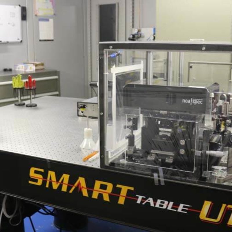
Microscópio s-SNOM e óptica de incidência da Linha de Luz IR1.
English:
s-SNOM microscope and incidence optics of the IR1 beamline.
Português:
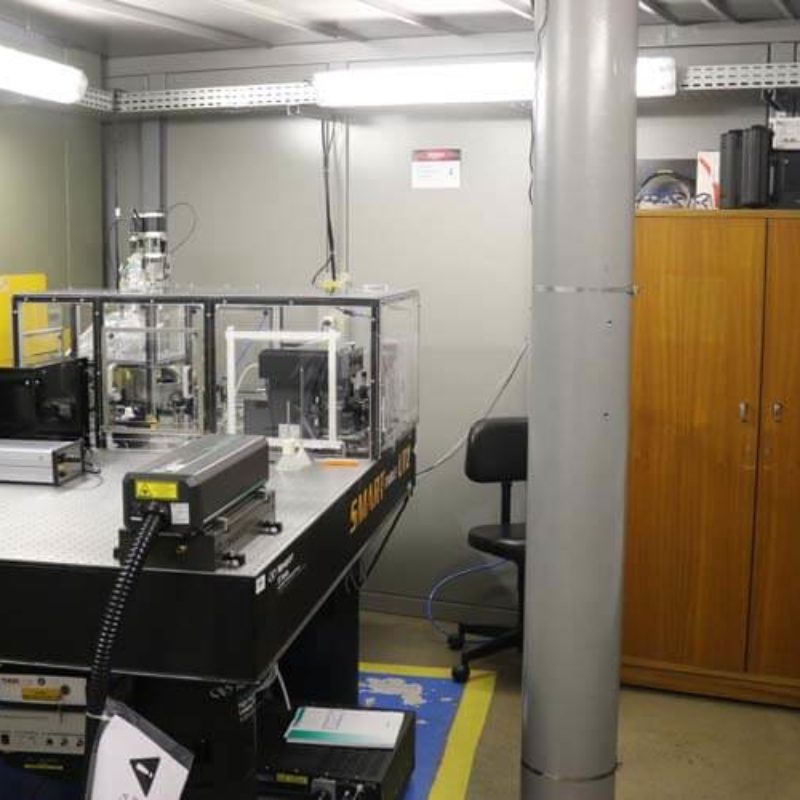
Estação experimental de nanoespectroscopia no Infravermelho.
English:
IR nanospectrocopy experimental station.
Português:
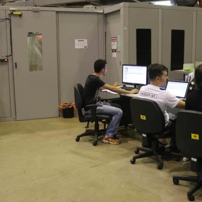
Mesas de controle experimental da linha de luz e estações de trabalho para processamento de dados para usuários.
English:
Beamline experiment control desks and data processing workstations for users.
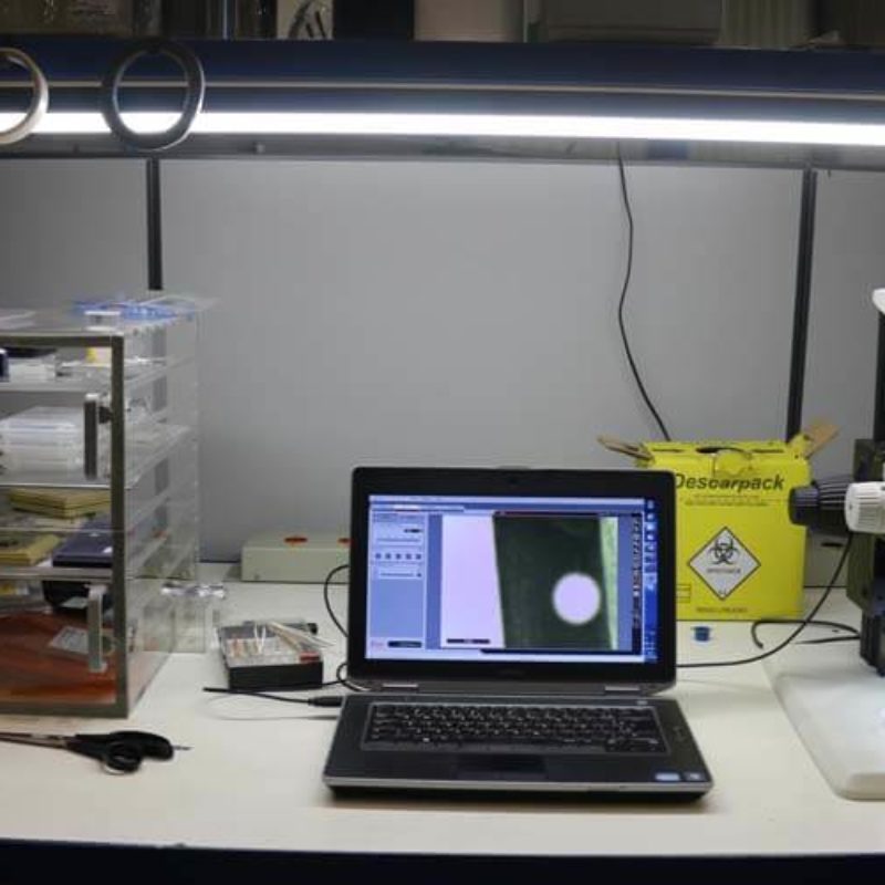
Português:
Bancada para preparação de amostras para usuários da Linha de Luz IR1.
English:
Sample preparation bench for users of the IR1 beamline.