

The small interface roughness and polarization phenomena lead to a larger charge-carrier mobility and better operational stability.
Recently, Muriel de Pauli et al (1) have shown that using a hybrid multilayer dielectric obtained by stacking successive $ rm Al_{2}O_{3}$/SAM bilayers can tailor interface phenomena and thereby significantly improve the charge-carrier mobility and operational stability of organic TFTs. While various groups have previously shown that hybrid inorganic/organic multilayer dielectrics are a powerful approach to producing gate dielectrics that cover a wide range of thicknesses (5–12 nm) and capacitances ($ rm 100-700,nF.cm^{-2} $), the influence of the number of inorganic/organic bilayers on the charge-carrier mobility and operational stability of the transistors was not explored yet. Through the use of alkylphosphonic acid SAMs with different chain lengths, the authors have revealed a threshold for the $ Al_{2}O_{3}$/SAM surface roughness; when the surface roughness is below this threshold, additional $ Al_{2}O_{3}$/SAM bilayers enhance the carrier mobility, otherwise additional bilayers will reduce the mobility.
In preparing hybrid multilayers one has to aim for an inorganic dielectric that can be deposited at low temperatures and provides atomically smooth interfaces. This is possible by using $ rm Al_{2}O_{3}$, obtained by the controlled reaction of $ rm Al (CH3)3 (trimethyl-aluminum) and water. Alkylphosphonic acids (PAs) are known to form high-quality self-assembled monolayers on the surface of atomic-layer-deposited $ rm Al_{2}O_{3}$ films. Figure 1a shows a view of the TFT structure based on an hybrid multilayer dielectric: the gate is made of doped silicon. Alkylphosphonic acid molecules with 3 distinct alkyl chain lengths of 1.3 nm (HC10-PA), 1.7 nm (HC14PA), and 2.1 nm (HC18-PA) were investigated in order to optimize the quality of the dielectric. The hybrid multilayer consists of an intercalation of $ rm Al_{2}O_{3}$ (9 nm) and solution-processed SAMs. The alkyl chain greatly influences the molecular packing within the SAM. One can obtain distinct multilayer structural properties due to a dependence of the resulting interface roughness with the presence of defects on the supramolecular packing (long-range order). Samples with a different number of $ rm Al_{2}O_{3}$/SAM bilayers were prepared, with the number of bilayers ranging from 1 to 6. 25 nm thick films of the small-molecule organic semiconductor dinaphtho [2,3-b:2′,3′-f]thieno[3,2-b]thiophene (DNTT), which has previously shown high carrier mobilities and good air stability, were deposited onto the multilayers. Source and drain Au contacts were finally deposited onto this organic semiconductor layer using shadow masks. The performance of these TFTs was evaluated and compared to devices fabricated with a single Al2O3/SAM bilayer dielectric. Measurements of the gate-dielectric capacitance, the transfer and output characteristics and the bias stress behavior were performed on all samples. Figure 1b shows the carrier mobility with different numbers of stacked $ rm Al_{2}O_{3}$/ SAM bilayers in which the SAMs are based on either HC10-PA (blue squares), HC14-PA (red circles), or HC18-PA (green triangles). The carrier mobilities were determined by fitting the measured transfer curves to the standard FET equation using the value of the gate-dielectric capacitance measured at a frequency of 100 Hz.
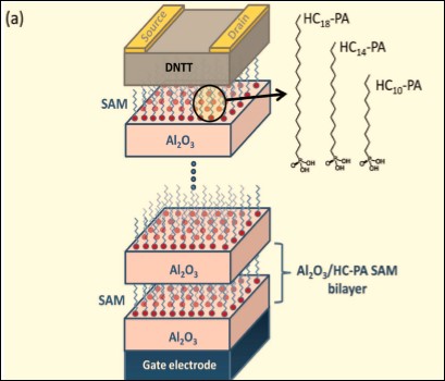
Figure 1. a) TFT fabricated using a hybrid multilayer dielectric composed of atomic-layer-deposited $ rm Al_{2}O_{3}$ layers with a thickness of 9 nm and alkylphosphonic acid SAMs. The molecular structures of the alkylphosphonic acids HC10-PA, HC14-PA and HC18-PA are also depicted. The number of stacked Al2O3/SAM bilayers ranges from 1 to 6.
To account for the fact that the TFTs with the large number of stacked $ rm Al_{2}O_{3}$/SAM bilayers have a larger gate-dielectric capacitance, these TFTs had to be operated with larger gate-source voltages in order to produce similar electric fields and similar charge-carrier densities in the semiconductor channel. To check whether the observed dependence of the carrier mobility on the number of stacked $ rm Al_{2}O_{3}$/SAM bilayers could be explained as a field-dependent carrier mobility in the context of multiple trapping and release (MTR) model, the authors fabricated and characterized a reference sample based on a single hybrid Al2O3/SAM bilayer consisting of a 62 nm thick layer of $ rm Al_{2}O_{3}$ and an HC14-PA SAM, thus having the same total dielectric thickness as in the TFTs with six $ rm Al_{2}O_{3}$ (9 nm) /HC14-PA SAM bilayers. A mobility of $ rm 3.3 ,cm^{2}.V.s^{-1}$ was measured in these TFTs. The carrier mobility for a single hybrid $ rm Al_{2}O_{3}$/ HC14-PA SAM bilayer is essentially independent of the $ rm Al_{2}O_{3}$ thickness. Therefore, this indicates that the characteristic dependence of the carrier mobility on the number of hybrid $ rm Al_{2}O_{3}$/SAM bilayers observed in Fig. 1b is not related to the total dielectric thickness or to the applied gate field, but to the number of inorganic/organic interfaces, their low roughess, polarization (discussed below) and its consequently larger DNTT grain size.
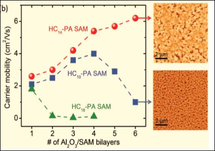
b) Charge-carrier mobility in function of the number of $ Al_{2}O_{3}$/SAM bilayers. Distinct dependencies of the carrier mobility on the number of $ rm Al_{2}O_{3}$/SAM bilayers are observed. The inset shows AFM images of the thin-film morphology of the organic semiconductor (DNTT) with six $ rm Al_{2}O_{3}$/HC14-PA SAM or six $ rm Al_{2}O_{3}$/HC10-PA SAM bilayers. The z-scale maximum was set to 90 nm in both images.
Atomic Force Microscopy
In order to clarify why the dependence of the carrier mobility on the number of bilayers is so different for the three phosphonic acids, the authors used atomic force microscopy (AFM) to study the thin-film morphology of the organic semiconductor films deposited onto the different HMDs. The differences in the DNTT grain size observed in these measurements are directly related to the differences in the carrier mobility. AFM topography maps of the surface of DNTT layers deposited onto six $ rm Al_{2}O_{3}$/HC14-PA SAM bilayers as well as onto six $ rm Al_{2}O_{3}$/HC10-PA SAM bilayers were studied. Stacking more bilayers substantially modifies the carrier mobility in the organic semiconductor layer deposited onto the HMD. An improvement in mobility is observed up to four bilayers in the case of the HC10-PA SAM, while for the HC14-PA SAM, the HMD surface roughness remains small (3.5 nm) and the DNTT grain size remains large (about 1.2 $ rm µ m) even for six bilayers. Such small roughness is unexpected for such a large number of stacked inorganic/organic bilayers.
Bias Stress Measurements
In order to understand the high carrier mobility in TFTs with multiple $ rm Al_{2}O_{3}$/HC14-PA SAM bilayer dielectrics, bias-stress measurements were carried out. It is known that charge trapping in the dielectric or at the semiconductor/dielectric interface results in a decrease in drain current. Hence, a monotonic decrease of the drain current would be expected for the TFTs. This behavior is clearly observed in the TFT with a single bilayer. However, the introduction of more than one bilayer causes an initial increase of the drain current during bias stress, followed by a decay that is slower for stacks with a larger number of bilayers. In the sample with five bilayers, the drain current continues to increase for the entire duration of the bias-stress measurement (60 min). The observed drain-current increase during bias stress in TFTs based on $ rm Al_{2}O_{3}$/HC14-PA SAM HMDs can be ascribed either to dielectric polarization or to charge injection from the gate. Since the gate current is very small ($ leq 10^{-11} A $), charge injection from the gate can be ruled out, so polarization effects must be the main reason for the observed drain-current increase. Such polarization may be enhanced by the presence of highly dipolar groups in the dielectric originating from incomplete chemical reactions during ALD, due to the low ALD growth temperatures
X-Ray Reflectivity
The authors have evaluated the interface roughness within the HMDs of all samples by X-ray reflectivity, which is a well-known technique for investigating the structure and interface quality of dielectric layers. These measurements were performed prior to the semiconductor deposition at the XRD2 beamline of the Brazilian Synchrotron Light Laboratory (LNLS). The results showed that the average roughness at the interfaces between adjacent bilayers within the $ rm Al_{2}O_{3}$/HC14-PA SAM HMDs is smaller than that in the HMDs based on the other two phosphonic acids. From the reflectivity curves, a dependence of the interfacial roughness on the number of bilayers was found. One can define for the DNTT based TFTs a threshold for the surface roughness of the topmost dielectric surface of about 5 nm. As long as the surface roughness of the topmost dielectric layer is smaller than this threshold, the addition of another Al2O3/SAM bilayer enhances the carrier mobility in the organic semiconductor, whereas when the surface roughness of the topmost dielectric layer is larger than such threshold, additional bilayers will lead to smaller mobility. The mobility-roughness trend discussed above is expected to have general validity, and the value of the surface roughness threshold will depend on the properties of the organic semiconductor, e.g., its molecular size, crystal structure, orbital overlap, etc. The interface roughness and polarization effects discussed in the previous paragraphs are the key factors for correlating the structural and electrical characteristics in order to provide a physical scenario that explains the observed enhancement in carrier mobility and operational stability of the TFTs with the $ rm Al_{2}O_{3}$/ HC14-PA SAM HMDs.
Conclusion
In summary, hybrid multilayer dielectrics composed of alternating layers of $ rm Al_{2}O_{3}$ prepared by atomic layer deposition and alkylphosphonic acid SAMs obtained from solution were employed as the gate dielectric of organic thin-film transistors. The small interface roughness and polarization phenomena lead to a larger charge-carrier mobility and better operational stability compared with TFTs based on simpler gate dielectrics. The results show that polarization occurs at the inorganic/ organic interfaces of the hybrid multilayer dielectrics and is more pronounced as the number of bilayers is increased. Reduced charge trapping effects are observed in devices with smoother interfaces, leading to improved operational stability. A 5 nm roughness threshold was found as the maximum value that allows for large DNTT grain size and provides mobility enhancement on our HMD-based TFTs. This optimal dielectric surface roughness range is applicable to DNTT-based devices, while a similar trend is expected to be found on other systems and must be investigated whenever the use of HMDs is envisaged for improving device performance.
Source: Pauli M. d., Zschieschang U., Barcelos I. D., Klauk H., Malachias A. Tailoring the Dielectric Layer Structure for Enhanced Carrier Mobility in Organic Transistors: The Use of Hybrid Inorganic/Organic Multilayer Dielectrics. Adv. Electron. Mater., 2: 1500402 (2016). DOI: 10.1002/aelm.201500402
New catalyst shows a potential for industrial applications requiring durability and high thermal stability.
Hexagonal-shaped Cu2Te nanodisks self-organize into a network of ribbons fully embedded in rr-P3HT thin films.