Researchers from CNPEM and collaborators demonstrate the potential of naturally abundant and low-cost minerals for application in nanodevices
The earth’s crust consists mostly of minerals called silicates, rocks composed mainly of the chemical elements silicon (Si) and oxygen (O). This is the case of feldspar, whose erosion gives rise to clays; and quartz, the main component of sand, among others. Extremely abundant, silicates are used not only in the production of construction materials, glass, and ceramics, but also in agriculture, and in the pharmaceutical, cosmetic, chemical, and petrochemical industries.
Silicates are differentiated by the ratio between the number of silicon and oxygen atoms. This proportion determines how these and the other atoms that compose the mineral are distributed in space, called crystalline structure. In turn, this structure determines the mineral’s physical and chemical properties, and consequently its possible applications.
An important class of these minerals are the phyllosilicates, which have the proportion of 2 silicon to 5 oxygen atoms in their composition. This proportion makes their most stable structure be the stacking tetrahedral layers of silicon as the central atom and oxygen at the vertices, forming a hexagonal silicon lattice. These silicon tetrahedral layers are interspersed with octahedral layers of bivalent central atoms, such as magnesium, or trivalent, such as aluminum, containing oxygen and hydroxyls at the vertices.
Allied to the electrically insulating character of phyllosilicates, their structure allows insulating materials with few atomic layers to be easily obtained by mechanical exfoliation, just as graphene can be obtained from graphite.
Insulators of a few atomic layers with suitable properties are fundamental for the fabrication of electronic devices at the nanoscale. However, research in this direction is highlighted by the use of synthetic materials such as hexagonal boron nitride (hBN). As phyllosilicates are naturally abundant and easy to extract, the possibility of being used as insulators in the manufacture of nanodevices is of great interest, since the cost associated with the manufacture of these devices can be reduced compared to the use of synthetic insulators, favoring large-scale production.
However, since these are natural materials, chemical elements such as iron (Fe) and manganese (Mn) present in the environment during the mineral’s geological formation are incorporated into their structure. Called impurities, these atoms can play an important role in the material’s physical-chemical properties. In order to optimize the use of phyllosilicates in this type of technology, it is, therefore, necessary to thoroughly investigate their properties in the few-layer form, focusing mainly on understanding how impurities can influence the mineral’s properties and how they can be manipulated to obtain the adequate properties.
This is the work that researchers from the Brazilian Center for Research in Energy and Materials (CNPEM), and collaborators from institutions in Brazil and Japan, have been developing, resulting so far in the publication of two articles in journals of impact in the area. The work presents a systematic study of the properties of a few layers starting from the bulk properties of two phyllosilicates, called clinochlore and phlogopite, with the care to understand how the impurities present in these minerals influence their macroscopic properties.
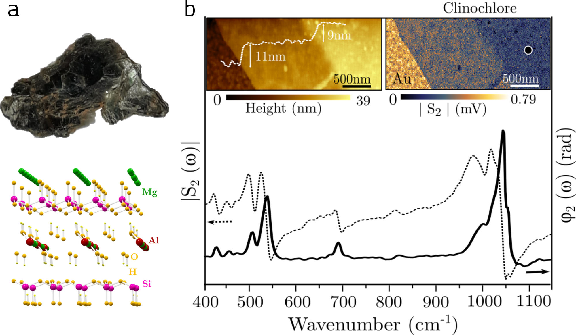
In work published in the journal Applied Surface Science [1], the researchers conducted a robust investigation of the mineral clinochlore, from the chlorite family, and its structural and spectral characteristics of few-layer and bulk forms.
Through various experimental techniques, including using synchrotron light, accompanied by a theoretical study, the group demonstrated that the incorporation of manganese (Mn) and chromium (Cr) impurities occurs homogeneously in the mineral, while iron (Fe) impurities can also be incorporated in the form of inclusions. Furthermore, the study showed that iron impurities are mainly responsible for the reduction in the optical bandgap of the material, i.e., in its insulating capacity. It was also observed that clinochlore maintains its lattice vibrational properties when reduced from many to few atomic layers by mechanical exfoliation, being possible to obtain ultra-thin layers of clinochlore with atomically flat surfaces comparable to hBN.

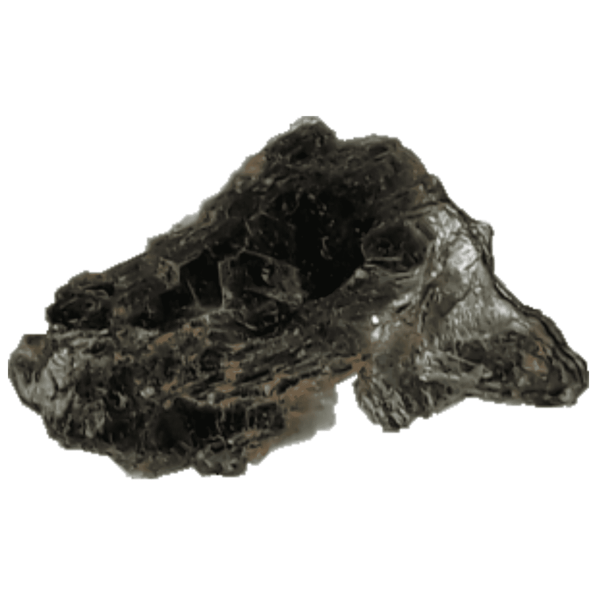
Figure 1: (a) Photograph of the natural crystal and crystal structure of clinochlore, (b) AFM (top right) and infrared (top left) images and (bottom) nano-FTIR spectrum obtained on few atomic layers of the material.
In the article published in the journal 2D Materials [2], the study of phlogopite, a phyllosilicate of the mica family, was performed in the few-layer and bulk forms, similar to the study performed with clinochlore.
In addition, the researchers evaluated that the ultrathin flakes of phlogopite obtained by mechanical exfoliation are stable when exposed to air and temperature variations and can be used in the manufacture of nanodevices formed by stacking atomic layers of different lamellar materials, called van der Waals heterostructures. The group demonstrated that the efficiency of excitonic recombination, when bound electrons and holes recombine and emit light, in monolayers of WS2 on phlogopite is at least three times higher than on SiO2 substrates, similar to the efficiency obtained for monolayers of the same material on hBN.

Figure 2: (a) Photograph of the natural crystal and (b) crystal structure of phlogopite, (c) XRF mapping in a region and an isolated Fe island in the phlogopite crystal, (d) optical microscopy image of a van der Waals heterostructure.
Both works take the first step in the direction of using clinochlore and phlogopite in interesting nanotechnologies, reinforcing that naturally abundant minerals are viable low-cost alternatives for the fabrication of nanodevices and that remain little explored. Nature reserves us pleasant surprises, often what we are looking for is already literally under our feet, we just need to learn how to manipulate it.
Carnauba
The studies presented were two of the first scientific papers published with data obtained from the Carnauba beamline, one of the first research stations to start operating in the synchrotron light source Sirius at CNPEM.
The different experimental techniques available in this type of infrastructure allow the observation of microscopic aspects of materials, such as the atoms and molecules that constitute them, their chemical states and spatial organization, in addition to following the evolution in time of physical, chemical and biological processes that occur in fractions of a second.
The Carnauba beamline is Sirius’ longest, at 150 meters long. The large distance between the X-ray source and the sample allows a synchrotron light beam to be produced with a focus of only 30 nanometers. This allows analyses of the most diverse nano-structured materials to be performed, aiming to obtain 2D and 3D images with nanometer resolution, with benefits for materials sciences and nanotechnology, life and environmental sciences, or even archaeology and paleontology.
Source:
[1] Raphaela de Oliveira, Luis A.G. Guallichico, Eduardo Policarpo, Alisson R. Cadore, Raul O. Freitas, Francisco M.C. da Silva, Verônica de C. Teixeira, Roberto M. Paniago, Helio Chacham, Matheus J. S. Matos, Angelo Malachias, Klaus Krambrock, Ingrid D. Barcelos, High throughput investigation of an emergent and naturally abundant 2D material: Clinochlore, Applied Surface Science, 2022, 153959. DOI: 10.1016/j.apsusc.2022.153959
[2] Alisson R. Cadore, Raphaela de Oliveira, Raphael Longuinhos, Verônica de C Teixeira, Danilo A. Nagaoka, Vinicius T. Alvarenga, Jenaina Ribeiro-Soares, Kenji Watanabe, Takashi Taniguchi, Roberto M. Paniago, Angelo Malachias, Klaus Krambrock, Ingrid D Barcelos, Christiano J. S. de Matos, 2D Materials, 9, 035007. DOI: 10.1088/2053-1583/ac6cf4
Study elucidates unprecedented processes of herbivore metabolism involved in the efficient degradation of plant fibers
Paper presents multiscale (nano-micro) FTIR analysis applied to the investigation of the chemical processes in Li-Air batteries