Researches look for new materials for extreme ultra-violet lithography.
Cellphones, computers and other omnipresent portable electronic devices owe their existence to the continuous miniaturization of electronic circuits, which begun with the invention of the transistor, in 1947. Responsible for turning on and off or amplifying an electrical current, the transistors replaced the big and fragile vacuum tubes that made the first digital computers occupy whole rooms of even whole buildings.
Another contribution to the production of smaller and smaller devices was the development of the integrated circuits. The components of these circuits – transistors, resistors, capacitors, and diodes – are sculpted directly into a silicon substrate using ultraviolet light. Today they are composed of millions of transistors per square millimeter and this number roughly doubles every 24 months.
The bigger the density of transistors and other components in a circuit, the smaller is the wavelength of ultraviolet light necessary for their production. For that, the development of new materials and processes that are compatible with higher energy radiation is necessary.
Thus, researchers from the Federal University of Rio Grande (FURG) and Federal University of Rio Grande do Sul (UFRGS), both in Brazil, and from the Indian Institute of Technology Mandi, in Himachal Pradesh, India, used the Brazilian Synchrotron Light Laboratory (LNLS) facilities to investigate the properties of new polymers for the production of the next generation of integrated circuits.
Integrated Circuits
Since the end of the 1970s, integrated circuits are produced through a technique called photolithography, which consists in the transference of a geometric pattern to a substrate using light.
Standard integrated circuits use thin slices of an extremely pure silicon crystal as substrate, over which a thin layer of silicon oxide and a thin film made of photosensitive polymers are deposited. The ensemble is irradiated by UV light according to the pattern defined by an optical mask and the polymers chemical bonds are broken and rearranged by the radiation. Then, it goes through a development process that selectively removes the photosensitive material.
Next, the silicon is subjected to the so-called doping process: the addition of impurities to a semiconductor material to change its electrical properties. Insulator and conductor material can also be included to produce the different elements of the circuit. The higher the density of such components in the circuit, the smaller must be the wavelength of the radiation used.
Extreme ultraviolet photolithography
Until the 1990s, ultraviolet light of 437, 405, 365 and 313 nanometers were employed in photolithography. At that time, new materials and processes allowed lowering the wavelength to 248 nanometers and again, in the turn of the century, to 193 nanometers, into the deep ultraviolet region. The new frontier lies in the extreme ultraviolet radiation, in the 12.5 nanometer region.
Light with such small wavelength is ionizing, producing a large amount of secondary electrons upon interaction with matter. These electrons can damage the non-exposed areas, compromising the quality of the circuit. Hence, the development of new polymeric materials and the understanding of their photodynamic properties – the way they behave under irradiation – is necessary for the production of the new generation of integrated circuits.
New materials

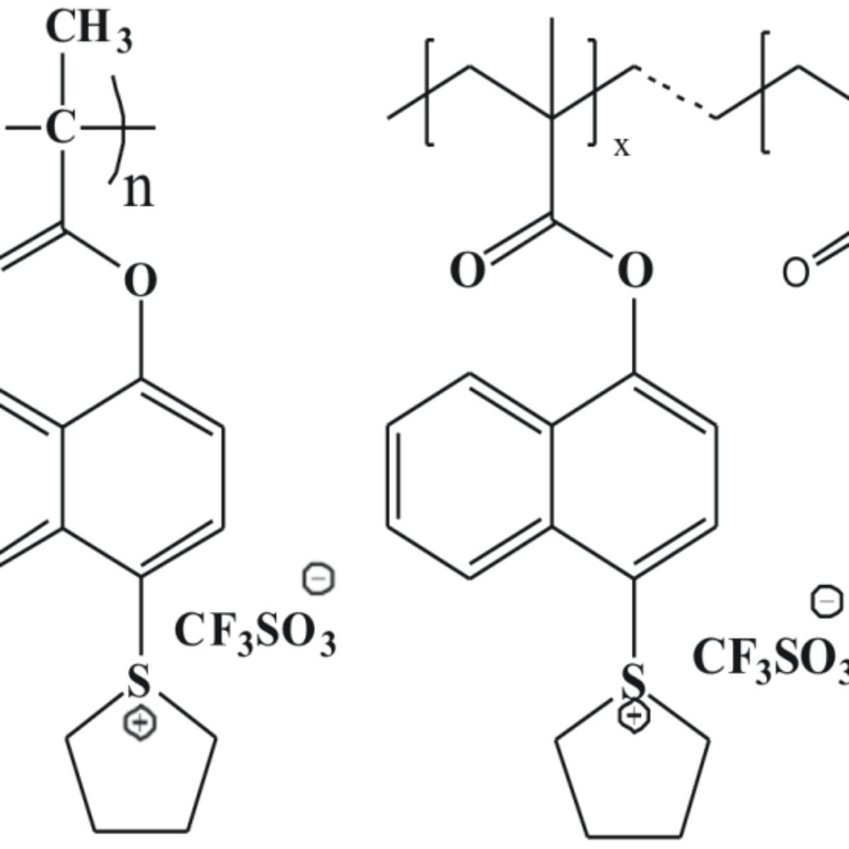
Figura 1: Representation of the homo- (left) and copolymer (right).
The scientists synthetized two different materials: a polymer obtained from molecules of the substance 1-(4-methacryloyoxy)naphthalene-1-yl)tetrahydro-1H-thiophenium trifluoromethanesulfonate or, in short, MANTMS and a copolymer obtained by addition of methyl methacrylate, MANTMS-MMA.
Thin films of both polymers were prepared and exposed to extreme ultraviolet light in the LNLS’ SGM beamline. According to the corresponding author, Daniel Eduardo Weibel, “the unique characteristics of the synchrotron radiation – high monochromaticity and intensity, and continuously variable energy – allows the acquisition of detailed information on the photofragmentation mechanisms, that is, the release of fragments that happens after absorption of photons on the extreme ultraviolet”. The investigation of the photodynamic properties of each polymer revealed that the copolymer MANTMS-MMA presented better stability due to the presence of the methacrylate group, capable of better dissipating the radiation’s energy as shown in Figure 2.
In addition, through the high monochromaticity of the synchrotron light source, the dependency of the photodynamic process with the excitation energy was studied. “Through the selective choice of excitations found in certain chemical reactions in the polymeric structure, it was possible to know the probable fragmentation mechanisms”. An important result is the possibility of selectively breaking the double bonds between carbon atoms in the polymers’ aromatic groups while keeping intact the bonds between carbon and oxygen, and carbon and fluorine atoms, making it possible to sensitize the material without producing gases, which can contaminate the circuit and compromise the manufacture.
The results also show the importance of choosing specific functional groups in the development of the new photosensitive polymers for the photolithography in the extreme ultraviolet and thus the production of smaller transistors and denser integrated circuits.
The research was supported by the Conselho Nacional de Desenvolvimento Tecnológico (CNPq) and Coordenação de Aperfeiçoamento de Pessoal de Nível Superior (CAPES).
Source: G.R. Chagas, V.S.V. Satyanarayana, F. Kessler, G.K. Belmonte, K.E. Gonsalves, and D.E. Weibel, Selective Fragmentation of Radiation-Sensitive Novel Polymeric Resist Materials by Inner-Shell Irradiation, ACS Applied Materials & Interfaces 2015, 7, 16348−16356. doi:10.1021/acsami.5b03378.
Researchers look for substitutes extracted from sunflower oil
Learning about its optical properties